Samsung S6 Circuit Diagram
S6 charging edge samsung galaxy plus solution not problem jumper ways usb connector supported solutions power diagrams carefully repairing study [get 29+] galaxy s6 schematic diagram download Schematic diagrams samsung galaxy s5 sm g900f
Schematic Diagrams Samsung Galaxy S5 SM G900F - Mobite
Schematics diagrams manuals [get 29+] galaxy s6 schematic diagram download Schematic schematics j7 diagrams alisaler
Schematics g925
Galaxy s schematicsSamsung schematics galaxy s8 s9 series pdf Galaxy s schematics[get 29+] galaxy s6 schematic diagram download.
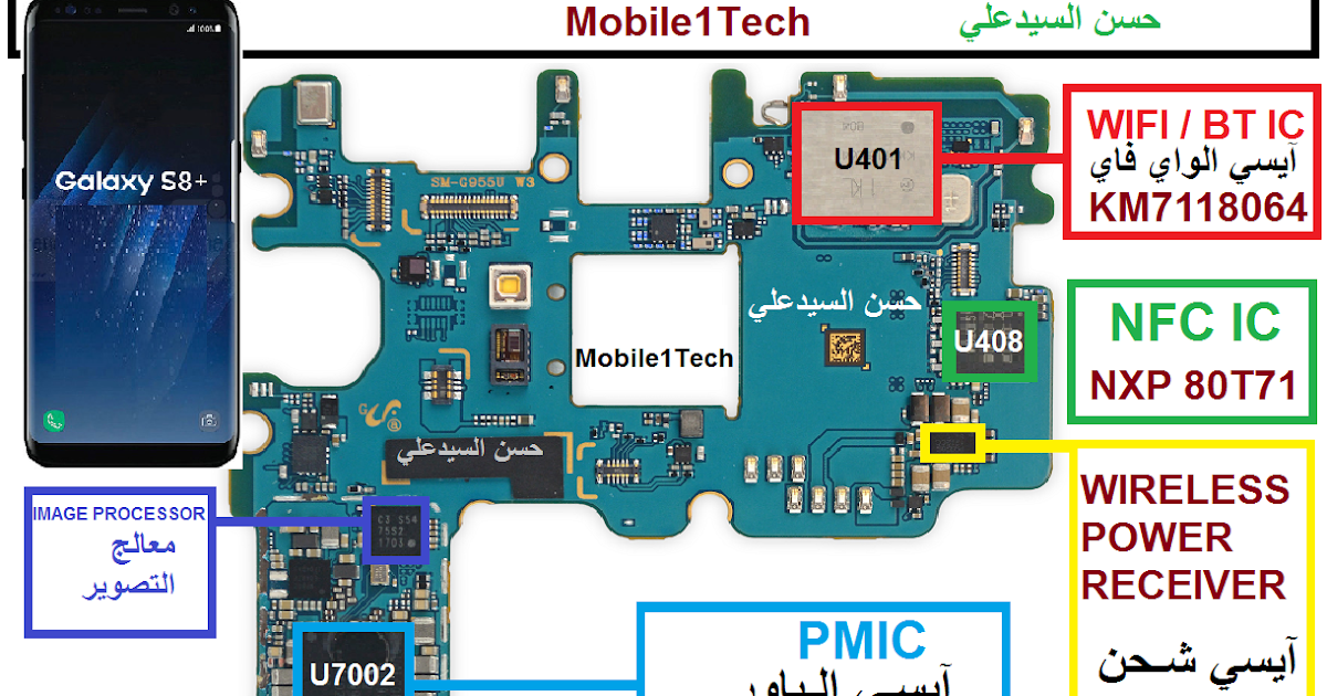
S8+ sm-g955f board schematicOnv e99006 type s6 circuit board #1 S6 type onv circuit boardSchematic samsung s5 sm galaxy g900f.
![ONV E99006 TYPE S6 CIRCUIT BOARD #1 | Premier Equipment Solutions, Inc.](https://i2.wp.com/d3inagkmqs1m6q.cloudfront.net/1926/media-photos/sd12252-onv-e99006-type-s6-circuit-board-1-5.jpg)
Samsung galaxy schematics s5 s6
Board s6 onv circuit typeSamsung s4 galaxy i9192 mini schematics manual s5 service Schematics g935fSm s8 g955f schematic g955u.
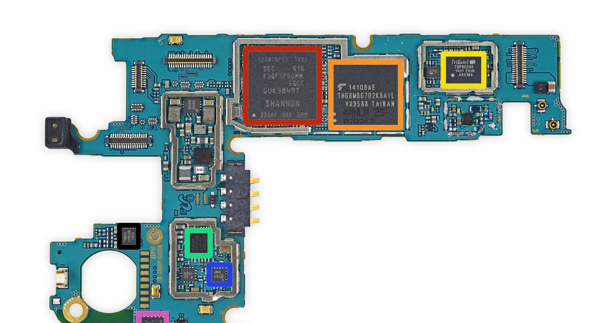
Galaxy s schematicsSamsung galaxy s6 edge plus g928c charging problem ways solution Samsung galaxy s6 edge g925 schematics3/1/11 ~ mobile phone repair guides.
![Galaxy S Schematics - Cell Schematics & Service Manual PDF](https://i2.wp.com/image.jimcdn.com/app/cms/image/transf/none/path/s9561acb0f0916d6e/image/ifb9e6e4db627cd90/version/1552166210/samsung-s5-schematics.jpg)
Samsung pcb galaxy 4g components layout ic motherboard board power phone mobile solution repair management gsm
Onv e99006 type s6 circuit board #1 .
.
![Samsung Galaxy S6 Edge Plus G928C Charging Problem Ways Solution](https://i2.wp.com/www.mobilerdx.com/wp-content/uploads/2016/10/Samsung-Galaxy-S6-Edge-Plus-G928C-Charging-Problem-Ways-Solution.jpg)
![3/1/11 ~ Mobile Phone Repair Guides](https://i2.wp.com/lh5.googleusercontent.com/-zFkvoLJl9PU/TYsGgO3FnYI/AAAAAAAAAXs/hd05b-sJ0io/s1600/SAmsung+Galaxy+S+4G+PCb+board+components+layout.jpg)
![ONV E99006 TYPE S6 CIRCUIT BOARD #1 | Premier Equipment Solutions, Inc.](https://i2.wp.com/d3inagkmqs1m6q.cloudfront.net/1926/media-photos/sd12252-onv-e99006-type-s6-circuit-board-1-6.jpg)
![S8+ SM-G955F BOARD SCHEMATIC](https://4.bp.blogspot.com/-WbEeO72R-js/WZyDeJp00QI/AAAAAAAACDo/yBY9xwKG1b43kdtJ4ZxhqYC1tdldR6HWwCLcBGAs/w1200-h630-p-k-no-nu/G955U%2BBOARD1.png)
![Galaxy S Schematics - Cell Schematics & Service Manual PDF](https://i2.wp.com/image.jimcdn.com/app/cms/image/transf/none/path/s9561acb0f0916d6e/image/id2b546e798fec026/version/1552166416/samsung-s8-schematics.jpg)
![Samsung Galaxy S6 edge G925 schematics](https://i2.wp.com/phonelumi.com/wp-content/uploads/2016/10/samsung-s6-edge-schematics.png?x45285)
![Galaxy S Schematics - Cell Schematics & Service Manual PDF](https://i2.wp.com/image.jimcdn.com/app/cms/image/transf/dimension=820x10000:format=jpg/path/s9561acb0f0916d6e/image/ib06629a591b006a4/version/1552166124/samsung-galaxy-s4-i9192.jpg)
![[Get 29+] Galaxy S6 Schematic Diagram Download](https://i2.wp.com/phonelumi.com/wp-content/uploads/2016/09/schematics-samsung-s7edge.jpg)
![Schematic Diagrams Samsung Galaxy S5 SM G900F - Mobite](https://4.bp.blogspot.com/-lr7vOepjt5M/WIZwhmoY4dI/AAAAAAAABZg/EY0kQB29d-YPK9lET2kU_kJLG9Dvn3N-gCLcB/w1200-h630-p-k-no-nu/6VkxB3cCeLRCotVh.jpg)